Practise 16 exam-style questions on Material removal for AQA GCSE Engineering. Write your answer as you would in the exam and get it marked in seconds against the mark scheme, point by point, with the Study Helper on hand if you get stuck.
16 questions
1–8 marks each
Instant marking
No sign-up needed
16 questions, marked as you go
Sample questions with model answers
Here are 4 of the questions in this topic, each with a model answer, an explanation of why it earns the marks and the mark scheme an examiner would use.
Question 1
1 mark
Which of these cutting processes produces no swarf (chips)?
Choose your answer.
A Drilling
B Milling
C Sawing
D Shearing
Model answer
D Shearing
Explanation
In shearing, two blades pass close to each other and the sheet fractures along the line between them, so no material is removed as chips and there is no kerf. Drilling, milling and sawing all cut material away with teeth or cutting edges, producing swarf. This is why a guillotine is quick and wastes no material when cutting thin sheet in straight lines.
Mark scheme
1 mark
D / Shearing
Accept the letter or the option text. If more than one option is given, 0 marks.
Question 2
2 marks
Describe the difference between face milling and slot milling.
Model answer
Face milling machines a large flat surface across the top or face of the workpiece. Slot milling cuts a narrow groove, such as a keyway, of a set width and depth into the workpiece.
Explanation
Both are milling operations, but the result is different: face milling leaves a flat, level surface, while slot milling leaves a channel, often cut with a slot drill whose diameter equals the slot width. A full answer describes both processes; describing only one scores 1 mark.
Mark scheme
1 mark
Face milling: produces a flat (level) surface across the face of the workpiece
Accept 'skims the top surface flat' or 'machines a large flat area'.
1 mark
Slot milling: cuts a narrow channel, groove or keyway (to a set width and depth) into the workpiece
Award 1 mark if only one process is described correctly. Accept 'uses a slot drill or side and face cutter the width of the slot'.
Question 3
3 marks
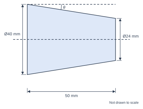
Figure 1 shows the tapered end of a component turned on a centre lathe. The diameter reduces from 40 mm to 24 mm over a length of 50 mm. The compound slide must be set to the angle θ shown.
Calculate angle θ. Give your answer to 1 decimal place.
Model answer
The radius changes by (40 − 24) ÷ 2 = 8 mm over 50 mm. tan θ = opposite ÷ adjacent = 8 ÷ 50 = 0.16 θ = tan⁻¹(0.16) = 9.1°
Explanation
The taper angle set on the compound slide is measured from the axis to one sloping side, so the opposite side of the right-angled triangle is half the change in diameter (8 mm), and the adjacent side is the length of the taper (50 mm). Use tan, because both sides you know are next to and opposite the angle. Forgetting to halve the 16 mm diameter difference doubles the answer.
Mark scheme
1 mark
Opposite side = (40 − 24) ÷ 2 = 8 mm; or a correct final answer of 9.1° with no working
An answer of 9.1° (or 9.09°) with no working scores 3 marks.
1 mark
tan θ = 8 ÷ 50 (= 0.16) / θ = tan⁻¹(8 ÷ 50)
Allow ECF from their opposite side, e.g. tan θ = 16 ÷ 50 (diameter difference not halved) scores this mark.
1 mark
θ = 9.1°
Accept 9.1° or 9.09°; 9.0° (incorrect rounding) does not score this mark. 17.7° (diameter difference not halved) scores 1 mark in total. sin⁻¹(8 ÷ 50) = 9.2° scores the first mark only.
Question 4
6 marks
Describe, in stages, how a printed circuit board (PCB) is made by photo-etching, starting from a circuit design and a sheet of photo-resist coated copper board.
Model answer
1. The circuit's track layout is drawn in PCB design software and printed in black onto a sheet of clear acetate to make a mask. 2. The photo-resist board is cut to size with a guillotine, and its protective film is peeled off in dim light. 3. The mask is placed on the board, printed side down, in a UV exposure box and exposed for about two minutes. The UV light passes through the clear areas and changes the resist there; the black tracks block it. 4. Wearing gloves and goggles, the board is put in developer solution. The exposed resist dissolves, leaving resist only on the track pattern. The board is rinsed in water. 5. The board is placed in warm ferric chloride in a bubble etch tank. The etchant dissolves all the copper that is not covered by resist. After about 15 minutes it is lifted out with plastic tongs and rinsed. Ferric chloride is corrosive and stains skin and clothes, so an apron, gloves and goggles are worn and the room is ventilated. 6. The remaining resist is rubbed off with wire wool to reveal the shiny copper tracks, which are checked for breaks or short circuits. 7. Finally, the component holes are drilled with a 1 mm drill on a PCB drill, wearing goggles.
Explanation
Top-level answers give the stages in order (mask, expose, develop, etch, clean, drill) with the equipment and chemicals used and the safety precautions, especially for corrosive ferric chloride and UV light. Students often confuse which copper is removed: the etchant removes the copper not protected by the resist. A list such as 'design, print, etch, drill' is capped at 2 marks.
Mark scheme
6 marks
Levels of response (6 marks). Level 3 (5-6 marks): Detailed explanation including all key stages to make the PCB, with the equipment used and safety. Notes are clear and in a logical order. Level 2 (3-4 marks): Some stages described in detail OR the majority of stages covered but with insufficient detail to allow correct manufacture. Level 1 (1-2 marks): One or more basic steps/stages listed. 0 marks: No response or nothing worthy of credit.
Max 2 if the stages are only listed with no detail. Indicative content, key stages in order (accept all other valid responses, including other etchants such as ammonium or sodium persulfate): 1. The track layout is designed with PCB CAD software and printed as a mask on clear film (acetate). 2. The photo-resist board is cut to size and its protective film removed in subdued light. 3. The mask is placed on the board in a UV exposure unit and exposed for a set time; UV light changes the resist that is not covered by the printed tracks. 4. The board is developed in a developer solution (e.g. sodium hydroxide), which dissolves the exposed resist and leaves resist on the track pattern; it is then rinsed in water. 5. The board is etched in ferric chloride solution, often warmed in a bubble etch tank, until all the unprotected copper has dissolved; it is removed with plastic tongs and rinsed. 6. The remaining resist is removed (e.g. with wire wool or a solvent) to reveal the copper tracks, which are checked for breaks and bridges. 7. Holes for the component leads are drilled with a small PCB drill (about 1 mm). Safety: ferric chloride is corrosive and stains, so wear gloves, goggles and an apron and use plastic tongs; work in a ventilated area; do not look at UV light; wear goggles when drilling; dispose of used etchant safely, not down the sink.
Ready to try the rest? Every answer you write is marked against the mark scheme, so you can see exactly where the marks are.
Ctrl + Enter to check
Study HelperHints first, answers after you try
Stuck on this one? Ask for a hint and I’ll point you in the right direction, without giving the answer away. Once you’ve checked your answer, I’ll show you how the marks are awarded.